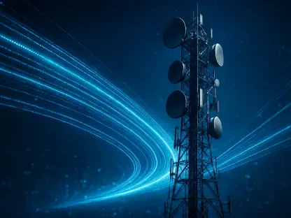

As a veteran networking specialist with a career spent dissecting the evolution of cellular, wireless, and next-generation connectivity, Matilda Bailey has observed the industry reach a critical inflection point. With AI workloads pushing traditional data center infrastructure to its physical and thermal limits, she is now focusing on Microsoft’s radical departure from conventional optical networking. By moving away from high-powered lasers and toward a massive parallel system powered by MicroLEDs, Bailey explores how this shift from “narrow and fast” to “wide and slow” could redefine the power dynamics of hyperscale clusters.
The following discussion explores the engineering behind this transition, including the use of medical-grade imaging fibers, the miniaturization of transceivers, and the strategic integration of hollow-core fiber to create a more efficient, sustainable backbone for the future of artificial intelligence.
Conventional networking relies on high-speed lasers, but using thousands of slower parallel channels via MicroLEDs represents a major shift. How does this “wide and slow” model impact signal integrity, and what specific architectural changes are required to manage such massive parallelism within a high-density server environment?
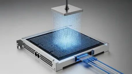
By moving to a “wide and slow” model, we are essentially trading the raw speed of a single channel for the collective strength of thousands. In traditional systems, pushing lasers to extreme speeds creates significant heat and signal degradation, but our internal testing shows that by distributing data across these parallel paths, we can maintain the same total bandwidth while cutting energy consumption by roughly 50%. Architecturally, this requires a fundamental redesign of how we interface with the chip, as we move away from a few precision-aligned laser beams to a dense array of commodity MicroLED emitters. It feels like moving from a single high-pressure water pipe to a massive, gentle showerhead; you get the same volume of water, but the individual components aren’t under nearly as much stress. This approach drastically simplifies the thermal management needs within the rack because we aren’t fighting the intense heat pockets typically generated by ultra-fast laser components.
Adopting imaging fiber—originally designed for medical endoscopy—is a unique approach to data transmission. What are the mechanical challenges of bundling thousands of light-guiding cores into a single cable, and how were you able to miniaturize the resulting transceiver into a thumb-sized form factor?
The mechanical feat here involves repurposing multi-core imaging fiber, which was perfected for medical use, to serve as a high-density data conduit. The primary challenge is ensuring that each of the thousands of light-guiding cores aligns perfectly with the MicroLED emitters on one end and the photodiodes on the other. We worked closely with partners like MediaTek to integrate these emitters, optics, and photodiodes into a cohesive unit that fits within a transceiver roughly the size of a thumb. Holding one of these prototypes feels like holding the future; it is incredible to see something so small managing a sea of data that would typically require much bulkier, more expensive hardware. This miniaturization is the “secret sauce” that allows us to plug these links directly into standard switches and servers without demanding a total overhaul of existing rack dimensions.
Reducing interconnect power by roughly 50% could fundamentally change how AI clusters are built. Beyond the energy savings, how does this technology alleviate the thermal constraints that currently limit GPU density, and what are the practical implications for the total cost of ownership in hyperscale facilities?
When you halve the power used by interconnects, you aren’t just saving on the electricity bill; you are removing a massive heat source from the heart of the server. Current AI clusters are often gated by their “thermal envelope,” meaning we can’t pack GPUs closer together because the networking hardware around them would literally melt or fail. By using cooler-running MicroLEDs, we can increase the density of our GPU clusters, allowing for more computing power in a smaller physical footprint. For a hyperscale operator, this translates to lower capital expenditure because we are using inexpensive, commercially available components rather than bespoke, costly laser systems. It shifts the total cost of ownership significantly, as the reduction in cooling infrastructure and energy usage makes “Green AI” a much more attainable reality rather than just a marketing slogan.
Short-range MicroLED links and long-distance hollow-core fiber address different layers of the data center network. How do these two technologies integrate within a single architecture, and what steps are necessary to ensure they work together seamlessly to eliminate performance bottlenecks during large-scale AI training?
These two technologies function as a “one-two punch” for the modern data center, with MicroLEDs handling the short-range, high-density traffic and hollow-core fiber (HCF) managing the long-haul connections. In an AI training environment, MicroLEDs eliminate the bottlenecks within the rack, while HCF provides a 47% faster transmission speed and 33% lower latency between different parts of the facility or between data centers. To make them work together, we are building a unified optical layer where the signal transition from one medium to the other is as transparent as possible to the software layer. This dual-pronged strategy ensures that whether a piece of data is traveling ten meters or ten kilometers, it is moving at the highest efficiency possible. It is about creating a holistic ecosystem where the physical limits of light propagation through glass or air no longer dictate the speed of our neural networks.
With commercialization targeted for 2027, what are the primary hurdles in moving this technology from a lab prototype to mass-market hardware, and how will your partnerships with component manufacturers help standardize this new cabling system across the industry?
The journey from a lab prototype to a mass-market product involves moving from high-precision manual assembly to high-volume automated manufacturing. We have to ensure that the ecosystem is ready, which means our partners must be able to produce these imaging fibers and MicroLED arrays at a scale that can support thousands of data centers worldwide. Standardizing the form factor is a huge part of this; by working with companies like MediaTek, we are ensuring that the industry sees this as a viable, plug-and-play alternative to traditional optics. The 2027 timeline is ambitious, but it gives us the necessary window to conduct long-term reliability testing outside of the controlled lab environment. We want to ensure that when a technician plugs in one of these cables in a humid or dusty data center, it performs with the same rock-solid reliability as the legacy fiber it replaces.
What is your forecast for MicroLED-based networking?
I expect MicroLED-based networking to become the cornerstone of the next generation of AI infrastructure, eventually replacing copper and traditional lasers for nearly all intra-rack communication. By 2030, the “wide and slow” architecture won’t just be an alternative; it will be the industry standard for any facility looking to balance the insatiable demand for FLOPS with the hard reality of power and thermal limits. We will see a shift where Microsoft and its partners own the underlying physical efficiency of the cloud, making their clusters not just the fastest, but the most cost-effective to operate. This technology will ultimately democratize high-density AI by lowering the entry barrier for building massive, energy-efficient training environments.