
The relentless pursuit of computational efficiency has reached a point where the speed of light itself is becoming a frustrating barrier to the real-time processing required for modern artificial intelligence systems. In the high-stakes race for AI supremacy, the greatest hurdle is no longer just raw processing power, but the physical distance data must travel across a motherboard. Every millimeter between a processor and its accelerator introduces a tiny delay that, when multiplied by trillions of operations, creates a massive performance ceiling. As Google and AMD join forces to fuse these components into a single package, the industry is shifting its focus from how fast a chip can think to how quickly it can communicate with itself.
This shift represents a fundamental change in hardware philosophy, moving away from the brute-force scaling of previous years. For years, the industry relied on increasing clock speeds and adding more cores to solve problems, but the bottleneck has moved to the interconnects. The current focus on internal chip communication highlights that the most advanced algorithms are only as fast as the electrical pathways they inhabit. By addressing this physical limitation, engineers are attempting to unlock a new tier of intelligence that feels instantaneous rather than calculated.
The Millimeter Gap Holding Back the Future of Artificial Intelligence
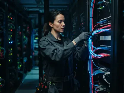
The physical layout of a modern server rack often reveals a hidden inefficiency that plagues even the most advanced neural networks. When a processor and an accelerator are separated by traces on a printed circuit board, the data must traverse a distance that, in the world of nanosecond computing, is equivalent to a vast desert. This separation forces the system to spend precious energy and time just moving information from the memory of one chip to the logic gates of another, creating a persistent drag on throughput.
As AI models grow in complexity, this “data tax” becomes increasingly expensive to pay. High-bandwidth memory and faster copper traces have provided temporary relief, but they do not solve the underlying issue of component isolation. The industry has reached a consensus that the only way to significantly move past current performance plateaus is to shrink the physical distance between the brain and the muscle of the computer. This involves a radical redesign of the silicon architecture to bring disparate functions into a unified, high-speed environment.
Why Latency Between Disconnected Chips Is the New AI Performance Ceiling
For years, the standard architecture for data centers involved pairing specialized Tensor Processing Units (TPUs) with traditional x86 CPUs. This discrete setup worked well for basic tasks, but the physical separation between the two creates a communication lag that stifles modern, complex models. As AI moves toward more interactive and autonomous behavior, the time wasted moving data back and forth has become a primary bottleneck, making the integration of general-purpose logic and AI acceleration a necessity rather than a luxury.
This latency issue is particularly visible in real-time inference where every millisecond counts for user experience. When a request must jump from a general-purpose processor to an accelerator and then back again, the overhead can account for a significant portion of the total response time. Furthermore, this disconnected approach limits the ability of the system to handle dynamic workloads that require frequent switching between different types of mathematical operations. The resulting inefficiency not only slows down the AI but also increases the power consumption of the entire data center.
Fusing General-Purpose Logic with Specialized Acceleration: The Hybrid Architecture
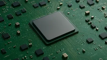
The collaboration between Google and AMD centers on a hybrid design that embeds CPU cores directly into the TPU processor package. This unified approach is specifically engineered to handle agentic AI and reinforcement learning, where a model must constantly check its work against general-purpose logic to refine its actions in real-time. By eliminating the need for data to exit the chip package, this architecture streamlines workloads that require a seamless blend of heavy-duty math and complex decision-making.
By placing the CPU and TPU on the same silicon substrate or within a 2.5D or 3D stacked package, the bandwidth between them increases by orders of magnitude. This allows for a shared memory pool, where both the AI accelerator and the general-purpose cores can access the same data without redundant copying. This integration effectively turns the entire package into a singular, versatile compute engine capable of handling the messy, unpredictable nature of human-like reasoning and logic-heavy AI agents.
Borrowing the Blueprint of Gaming Consoles for Next-Gen Data Centers
AMD’s role in this partnership is rooted in over a decade of perfecting Accelerated Processing Units (APUs) for the world’s most popular video game consoles. While competitors focused on standalone components, AMD mastered the art of merging CPUs and GPUs into high-performance, reliable systems for the Xbox and PlayStation. This deep expertise in custom silicon makes them the ideal partner for Google’s eighth-generation TPU efforts, proving that the future of hyperscale computing looks a lot like the integrated hardware found in a living room gaming setup.
The lessons learned from optimizing gaming hardware—where heat, space, and power are at a premium—are now being applied to the massive scale of the cloud. Gaming consoles required a balance of high-speed graphics and complex game logic to exist on a single chip to minimize latency during gameplay. This same principle is being used to build the next generation of custom AI accelerators, where the interplay between the TPU and the embedded CPU cores mimics the relationship between a console’s graphics engine and its main processor.
Preparing for Agentic AI: Strategies for a Unified Compute Future
The industry transitioned toward unified memory structures to mitigate the distance between processing elements and maximize data throughput. Developers embraced the Frozen v2 methodology, which prioritized token efficiency and low-overhead communication protocols to ensure that software remained compatible with the new hybrid silicon. These decisions reflected a shift in hardware philosophy that fundamentally altered how engineers approached large-scale AI deployments, moving away from fragmented systems toward cohesive, integrated environments.
Organizations successfully adapted by redesigning their stacks to leverage the reduced latency provided by the integrated Google and AMD architecture. Teams focused on ultra-efficient token management and prioritized frameworks that allowed for real-time reinforcement learning without the traditional communication penalties. This proactive approach ensured that as AI agents became more autonomous, the underlying hardware was capable of supporting the rapid-fire decision-making required for sophisticated digital reasoning. Overall, the shift toward integrated compute proved to be the decisive factor in overcoming the final barriers to seamless artificial intelligence.